Engineering Physics
Semiconductors & Superconductivity
Unit IV: Semiconductors & Superconductivity. This unit covers semiconductor band theory, charge carriers, PN junctions, diode and transistor action, followed by the essential physics of superconductors, key properties, the Meissner effect, critical parameters and the classification and applications of superconducting materials used in modern technology.
Basics of Semiconductors: Bands and Carriers
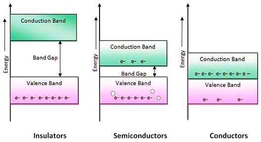
- Semiconductors have a narrow forbidden energy gap (≈ 1 eV) between the valence band and conduction band, unlike insulators (wide gap) or metals (overlapping bands).
- At absolute zero, the valence band is full and the conduction band is empty; thermal excitation promotes electrons across the gap at room temperature.
- Intrinsic semiconductors (e.g. Si, Ge) have equal electron and hole concentrations; extrinsic semiconductors are doped with donor (n-type) or acceptor (p-type) impurities to control carrier density.
- Conductivity σ = n e μe + p e μh, where n and p are electron and hole densities, and μ are their respective mobilities.
PN Junctions and Diodes
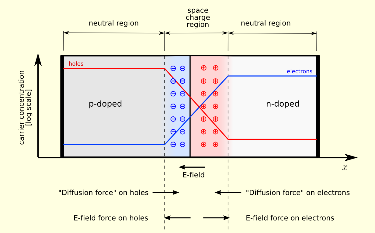
- A PN junction is formed when p-type and n-type semiconductors are brought together; diffusion of carriers creates a depletion region with a built-in electric field opposing further diffusion.
- Forward bias reduces the potential barrier, allowing significant current flow; reverse bias widens the depletion region, allowing only a tiny leakage current.
- The ideal diode equation is
I = I₀ [exp(eV/kT) - 1], where I₀ is the reverse saturation current. - Diodes are used as rectifiers, signal clippers, voltage references (Zener diodes) and light emitters (LEDs).
Transistor Action (Qualitative)
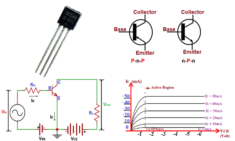
- A bipolar junction transistor (BJT) consists of two back-to-back PN junctions (NPN or PNP) with three regions: emitter, base and collector.
- The thin, lightly doped base allows most injected minority carriers to diffuse through and be swept into the collector, producing current amplification.
- Current gain β = IC / IB; a small base current controls a much larger collector current, enabling amplification and switching.
- FETs (Field Effect Transistors) control current via an electric field at the gate; MOSFETs are the fundamental switching element in all modern integrated circuits.
Phenomenon of Superconductivity
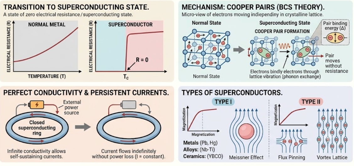
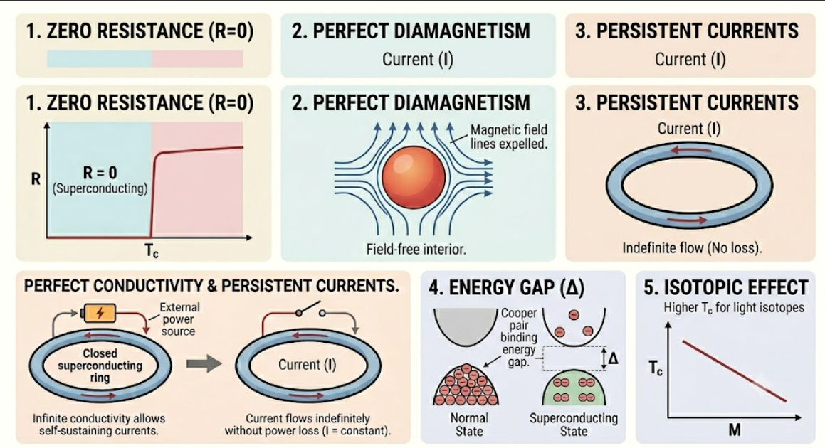
- Superconductivity is the state of certain materials in which electrical resistance drops to zero when cooled below a characteristic transition temperature Tc.
- Perfect conductivity results in persistent currents that can flow indefinitely without power loss.
- Transition to superconducting state is a phase change involving electron pairing (Cooper pairs).
- Occurs in metals, alloys and certain ceramics depending on material structure.
Properties of Superconductors
- Zero electrical resistance below Tc.
- Perfect diamagnetism indicating expulsion of magnetic flux from the interior.
- Persistent currents in closed loops with extremely long lifetimes.
- Energy gap in electronic density of states due to Cooper pairing.
- Isotopic effect showing dependence of Tc on atomic mass.
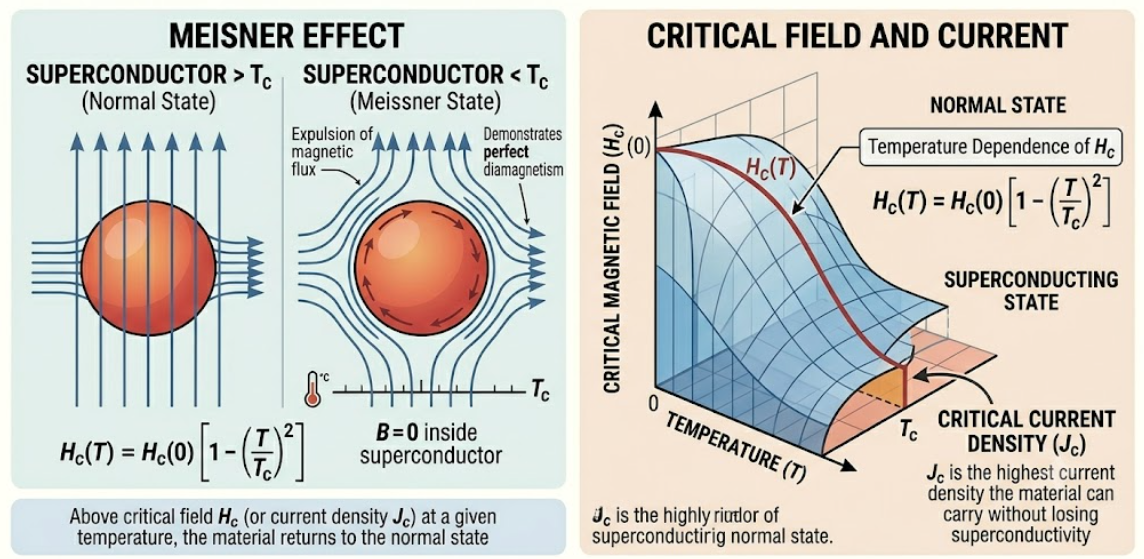
Meissner Effect and Critical Parameters
- Meissner effect is the complete expulsion of magnetic flux from a superconductor below Tc, demonstrating perfect diamagnetism.
- Critical magnetic field Hc is the maximum field below which superconductivity can exist. Above Hc the material returns to the normal state.
- Temperature dependence:
Hc(T) = Hc(0) [1 - (T/Tc)^2]. - Critical current density Jc is the highest current per unit area the material can carry in superconducting state.
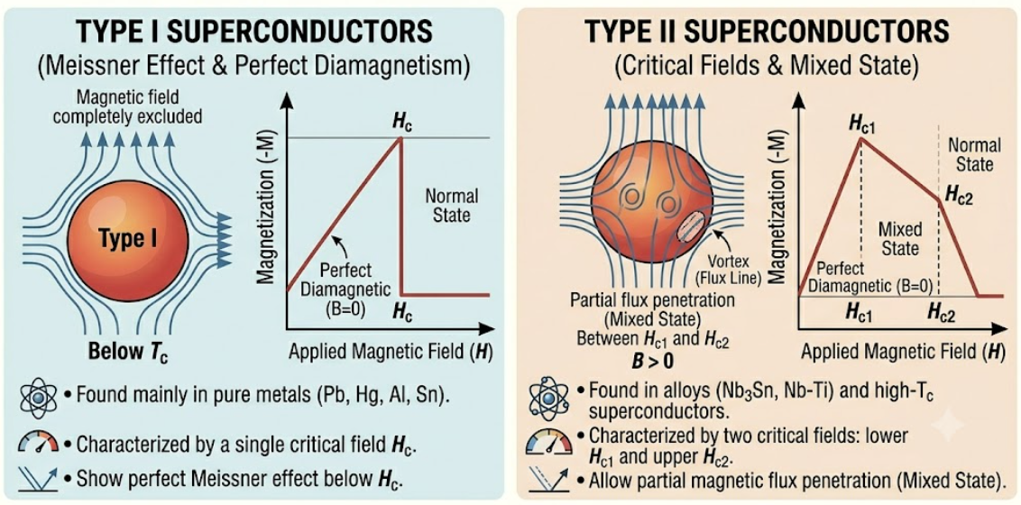
Types of Superconductors
- Type I Superconductors
- Show perfect Meissner effect.
- Single critical field Hc.
- Found mainly in pure metals like Pb, Hg, Al.
- Type II Superconductors
- Characterized by two critical fields Hc1 and Hc2.
- Allow partial flux penetration in mixed state.
- Found in alloys and high Tc superconductors.
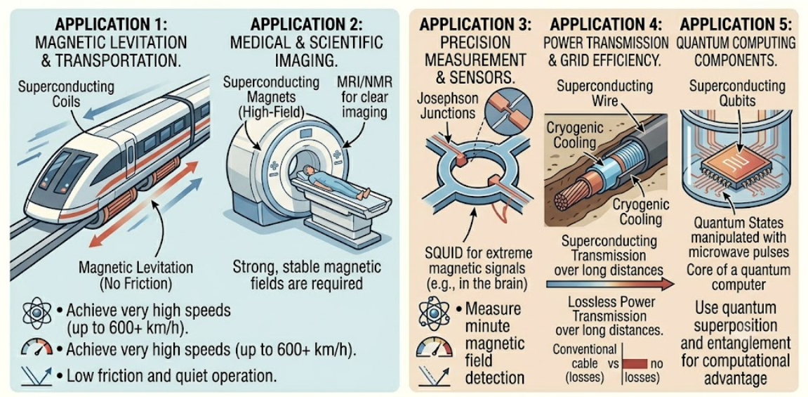
Applications of Superconductors
- Magnetic levitation and high speed maglev trains.
- Superconducting magnets for MRI and NMR systems.
- Josephson junctions and SQUIDs for precision measurement.
- Cryogenic power cables and lossless energy transmission.
- Quantum computing components based on superconducting qubits.
This unit covers semiconductor physics and superconducting materials together with their technological importance. If you need a one page revision sheet, ask for the Unit IV cheat sheet.
Ready to test your Chapter IV: Superconductivity knowledge?
Chapter IV: Superconductivity
A short module quiz for Chapter 4 covering superconductivity, Meissner effect, critical parameters, and applications.